
Vacuum solutions engineered for semiconductor & electronics
The industry whose dust surprises people twice — the pristine fab hides a toxic-and-chemical exposure ledger, and the same 'high-tech, surely inert' assumption hides genuinely combustible dusts, from fine silicon to the reactive-metal powders now feeding advanced packaging.
HEPA-Tested Filtration
Toxic and fine fractions retained
Contamination-Aware
Cleanliness and capture together
Static-Safe Practice
ESD discipline near devices
Built for the Fab
Wafer line to packaging
Explosion-Proof
Manufacturing specialists
1000+
Vacuums sold worldwide
USA
Designed & manufactured
Direct
Buy from the manufacturer
NFPA 660
ATEX / IECEx principles
Semiconductor & Electronics production process explorer
Every stage. Every challenge. The right vacuum solution.
Chip-making runs from raw silicon to finished package through a chain of processes, each with its own residue. Walk the stages — the hazards are rarely what the clean floor suggests.
Stage 01 — Crystal growth & wafer prep
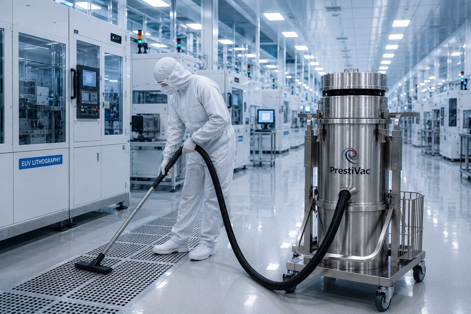
Slicing and grinding ingots produces fine silicon dust — a combustible particulate the 'high-tech means inert' assumption tends to miss. HEPA-retained recovery with ESD discipline from the very first step.
Key challenges
The dust the clean floor hides
Toxic Dopants & Metals
Arsenic, antimony and heavy-metal residues from doping and deposition are real exposure streams — the client's own framing: toxic and chemical hazards found in electronics.
Combustible Silicon
Fine silicon dust from ingot slicing and grinding is combustible — one of the dusts the 'surely it's inert' assumption most reliably misses.
Metal AM In The Fab
Advanced packaging brought reactive-metal powder-bed printing onto the electronics floor, with the combustible-metal rules riding along.
ESD Meets Dust
Devices demand electrostatic-discharge control, so recovery equipment must be static-safe as well as clean — two disciplines in one tool.
Contamination Is Yield
A fine particle is a killed die — housekeeping here is a yield input, so capture and cleanliness are the same objective.
Solder & Lead Streams
Assembly and rework shed solder dust and, in legacy lines, lead — toxic fractions demanding HEPA retention and sealed disposal.
Dust & materials knowledge center
Toxic, combustible, or both
Combustibility and severity are material- and particle-size-specific — testing and your Dust Hazard Analysis govern. Full directory: the full materials directory.
Applications in electronics
- PCB manufacturing
- Semiconductor fabrication
- Wafer processing
- Cleanroom production
- Electronics assembly
- Vacuum coating
- Display manufacturing
- Chip packaging
- SMT production
- View all
Built for performance. Built for compliance.
View all products →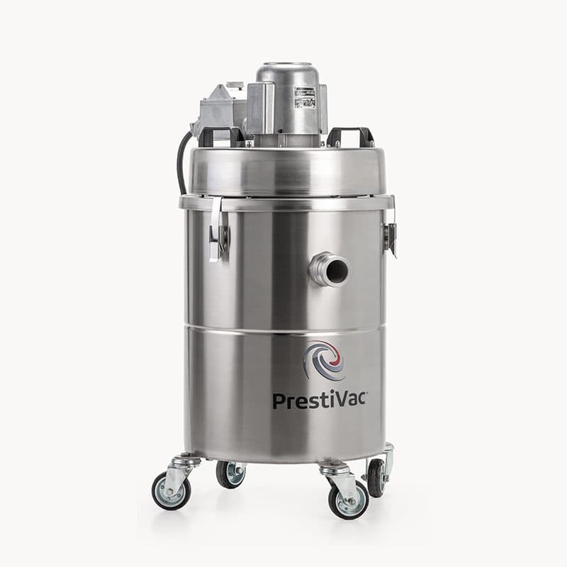
HEPA Vacuums
99.99% filtration for fine and hazardous dust
Learn more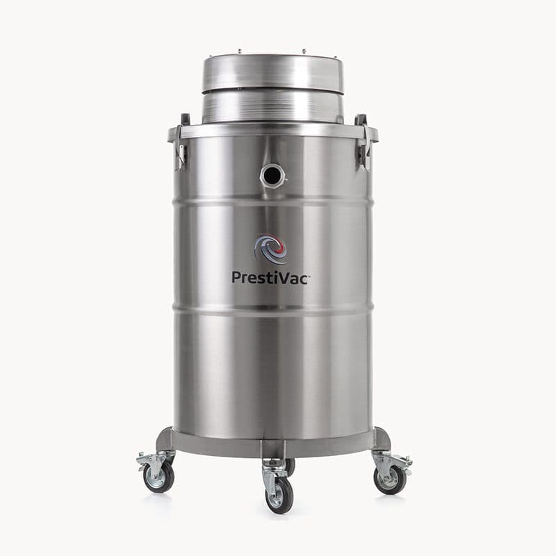
Explosion Proof Vacuums
Grounded, bonded recovery for combustible dust
Learn more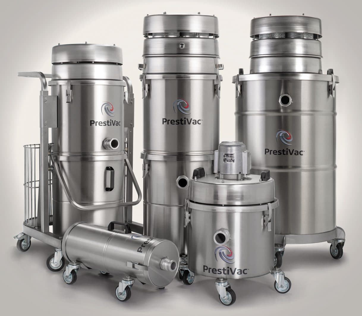
Industrial Vacuums
Continuous-duty recovery for demanding plants
Learn more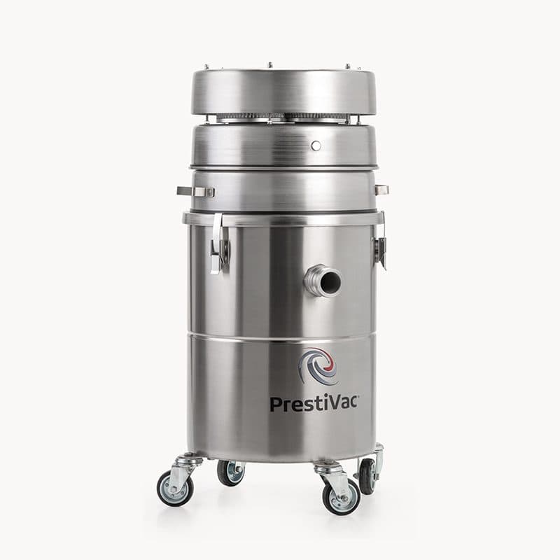
Central Vacuum Systems
Facility-wide housekeeping from fixed drops
Learn more
Representative case study
Dual-Hazard Dust Control in a Semiconductor &
How a representative advanced-electronics manufacturer runs housekeeping where the clean floor hides two hazard classes at once — toxic dopant, etch and CMP residues that are not combustible, and genuinely combustible dust the 'high-tech means inert' assumption misses: fine silicon from wafer grinding and the reactive-metal powder that advanced packaging brought onto the fab floor.
Read the full case studyTalk to the manufacturer
Get the right explosion proof vacuum for your application.
Tell us what you need to vacuum and where. Our technical team will recommend the PrestiVac model best suited to your material, your classification and how hard you will work it — and because we build every unit ourselves, we can modify it to fit.
- Legally certified explosion proof
- Solid stainless steel construction
- Industry-best 3-year warranty
- Designed & manufactured in the USA
- 200+ vacuum versions